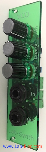
VCO: Voltage-controlled oscillator
Diagram
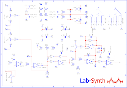
IC2A with the associated resistor and capacitor is a low pass filter on the Input. IC2B with the diode is a “super diode” to avoid any negative voltage at TP5. IC1A is an inverting amplifier with a shift tuned by trimmer R28.The idea is to obtain a strictly negative output at TP1. If this voltage is not strictly negative, the oscillator won’t oscillate. R28 adjust the minimum frequency. IC1D and IC1B are forming the oscillator. See hereafter the oscillograms corresponding to the test points TP2, TP3 and TP4 to visualize the operation of the oscillator. Finally, ICIC is an inverting amplifier.
Tuning the minimum frequency
Without anything at the Input, Coarse Offset (first) and Fine Offset (second) are tuned to obtain 0V at TP6. Afterward, the trimmer R28 is set to fix the minimum frequency (for example at 10Hz).
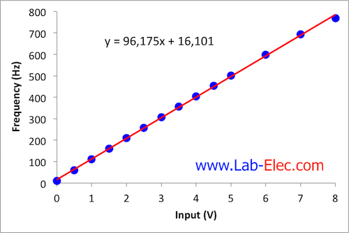
Result of some measurements
With 2.5V at the Input (Input pot at max), TP6 = 1.49V, TP5 = 1.49V and TP1 = -3.34V and the Output frequency is 258.2 Hz. With -2.5V at the Input (which make no sense), TP6 = -1.49V and TP5 = 0V.
Plot showing the link between the Input and the Output frequency
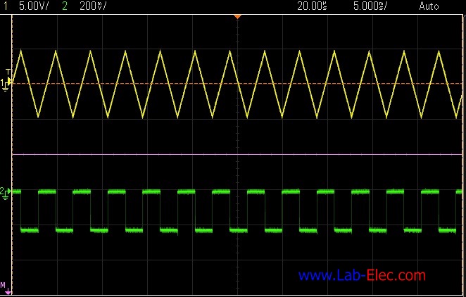
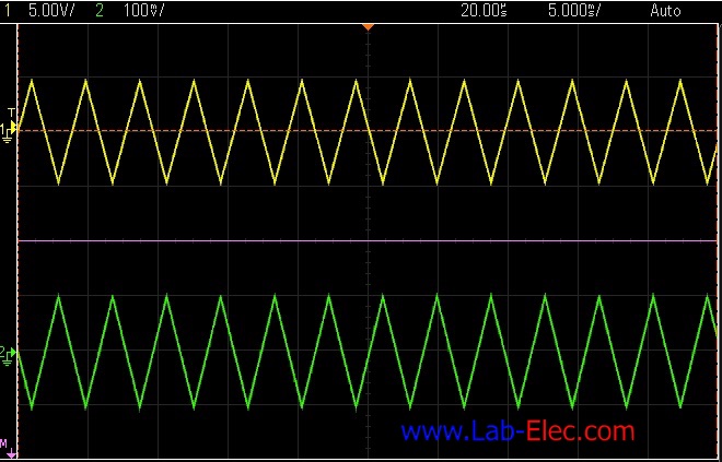
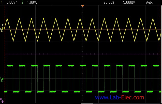
Oscillograms at the test points (Yellow is the Output)
Test point 2 (TP2)
TP3
TP4
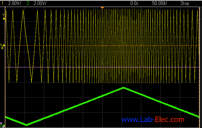
With a tringle at the Input
|